Shop Phones
Family
Compare
Motorola Razr
Motorola Edge
Moto G
ThinkPhone
All Smartphones
Compatibility
5G
On Sale
Family
Compare
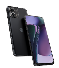
moto g stylus 5g - Free tablet
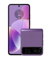
razr 2023 - Free Bose Earbuds
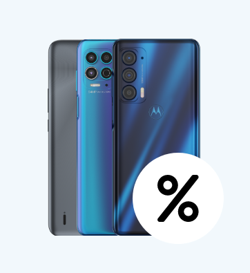
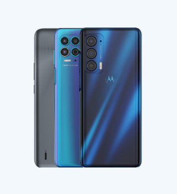
moto edge 2023 - $250 off
MOTO FEST SALE
Compare phones
Tablet
Business
Family
Compare
Moto for Business
$300 off ThinkPhone
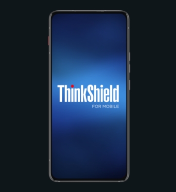
ThinkShield
Accessories
Family
Compare
Stylus Pens
Cases & Protection
Headphones
Wearables
Power & Charging
Satellite Link
Auto accessories
Smart Products
Family
Compare
Security & Surveillance
Modems + Routers
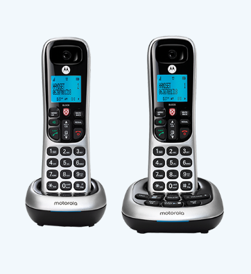
Home & Office Phones
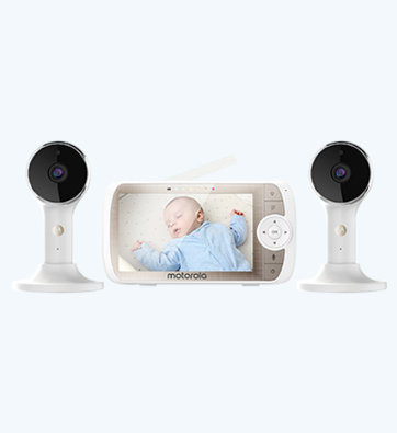
Smart Nursery & Monitors
Wearables
Tablets
Software & Support
Family
Compare
Support
Rescue & Smart Assistant
Software Updates
My UX
Beta Testing
Videos
Family
Compare
Motorola Videos
Services
Family
Compare
Moto Care
Screen Protect
Moto Parts
Sign In
B2B Inquiry
B2B Inquiry